The technology of Polytechnic University scientists will make the production of solar panels 30% cheaper
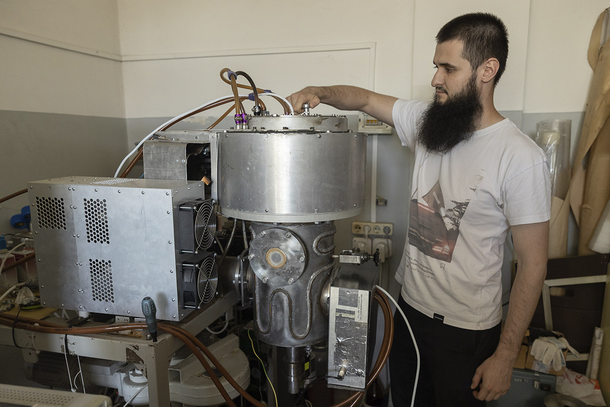
A research group from SPbPU has developed a technology for forming silicon nanostructures using nanosphere lithography and a plasma-chemical etching unit, which consists of 90% domestic parts. The technology will make production of solar cells cheaper by 30%.

Artyom Osipov, PhD in Technical Sciences, Head of the Scientific Research Laboratory «Technology of Materials and Electronic Products» of the SPbPU NTI Center, spoke about the essence of the project. Today, silicon is considered to be the main material in the semiconductor industry. Electric-vacuum devices and solar cells use silicon nanostructures — nano-rods and nano-needles. Their standard manufacturing method consists of several cycles, and each of them requires individual equipment, which makes production much more expensive. Scientists at St. Petersburg Polytechnic University have developed a unit for the production of nano-rods, in which all the necessary technological stages take place in a single cycle: the size, density, and height of the rods are controlled, and the mask (temporary protective coating) is removed.
The nano-rods produced in this way will find application in solar panels based on vertical transitions, which will make the production of solar cells cheaper by 30%.
The advantage of a vertical p-i-n-junction solar cell is that the sunlight, passing between the rods, is trapped and refracted several times, which increases its absorption coefficient and increases the efficiency of the solar cell
, explained Artyom Osipov, PhD in Engineering, Head of the Research Laboratory ‘Technology of Materials and Electronic Products’ of the SPbPU NTI Center. In addition, such vertical nanocells more effectively absorb scattered sunlight, so these panels work even in cloudy weather. The efficiency of a solar cell depends on the size of nanocells, which we select experimentally. To get the optimal values, we need to set the correct size and density of the structures. We can control these parameters in a single installation
.
The second result of the developed technology is silicon nano-rods, which are of particular interest for use in electro vacuum devices. These cold-cathode devices are used in satellite transmitters, tomographs, airplanes, communication centers, radio engineering, and television. Cold cathodes developed on the basis of silicon nano-needles exceed the current values of their existing analogues by 25%. Moreover, their lifetime is more than 40 times longer than the lifetime of thermal emission cathodes.
Plasma chemical etching unit for silicon nanostructures development was supported by the Priority-2030 Program of the Russian Ministry of Science and Technology.
The material was prepared by the Office of Strategic Planning and Development Programs. Text: Specialist of the Center for Analysis and Development Programs Polina Apolon
